


Chip Architectures
Defining and Describing Chip Architectures
_Chip architectures are the high‑level design choices that determine how a semiconductor chip organizes compute, memory, and data movement to deliver specific performance, power, and cost trade‑offs for a target market or workload.
[98hxl9]
[tmoau5]
[jxot1z]
*
For innovation work, the term applies when founders, investors, or product leaders are deciding what kind of chip (CPU, GPU, NPU, custom accelerator, 2D vs 3D, near‑memory vs off‑chip memory) is the right strategic substrate for their product or platform.
[98hxl9]
[tmoau5]
[jxot1z]
It does not apply to low‑level circuit implementation details (e.g., transistor sizing) or purely software concerns like cloud instance types, except insofar as those flow from architectural choices.
[98hxl9]
[t14wm9]
An innovation consultant cares because chip architecture decisions constrain product capabilities, unit economics, regulatory exposure, and long‑term differentiation: e.g., whether to ride commodity GPU roadmaps, license an existing ISA like Arm, or design a novel near‑memory or 3D architecture for AI or edge workloads.
[tmoau5]
[lyvgf0]
[jxot1z]
[l04l7i]
[v18ogx]
Disambiguation
Primary sense — the innovation-consulting sense
Definition (innovation sense):Chip architectures are the families of design decisions that define how a chip computes (e.g., CPU, GPU, NPU, 3D accelerator) and how it moves and stores data (e.g., on‑chip networks, memory hierarchies, stacking) to serve specific applications and business models.
[98hxl9]
[tmoau5]
[lyvgf0]
[jxot1z]
[t14wm9]
[v18ogx]
- In practice, this sense covers choices like “CPU vs GPU vs TPU‑style matrix units,” “flat 2D vs monolithic 3D stacking,” and “traditional von Neumann vs near‑memory compute,” all of which materially affect performance per watt, bill of materials, and feasible product experiences. [98hxl9] [tmoau5] [lyvgf0] [jxot1z]
- It is commonly used in trade press and talks to explain shifts such as “new chip architectures for AI at the edge,” where presenters describe pairing legacy CPU/DSP cores with specialized NPUs and near‑memory compute blocks to hit tight power and latency budgets. [tmoau5]
Other senses
1. Policy & macro sense — “chip architectures under sanctions”
Definition:Use of “chip architectures” in policy and economics to describe which design styles (e.g., GPU‑like accelerators, advanced AI architectures) are restricted or incentivized by export controls and industrial policy.
[st4bw4]
- Academic work on “Chip Architectures Under Advanced Computing Sanctions” analyzes how export controls target specific architectures (e.g., high‑bandwidth GPU‑class accelerators), and how those constraints reshape both architectural choices and economic outcomes. [st4bw4]
- For innovation consultants working in geostrategically sensitive markets, this sense matters because architectural choices (e.g., designing around sanctioned GPU configurations) directly affect market access, supply‑chain risk, and compliance. [st4bw4]
2. On‑chip communication architectures
Definition:A more specialized sense where “chip architectures” refers primarily to on‑chip communication architectures—the networks‑on‑chip and interconnect schemes that move data between cores, memory, and accelerators in a system‑on‑chip.
[t14wm9]
- A dedicated reference text describes “on‑chip communication architecture design” for system‑on‑chip interconnects, covering buses, crossbars, and complex networks‑on‑chip. [t14wm9]
- This sense is relevant to innovation when startups design highly parallel AI or networking chips where communication bottlenecks, rather than raw compute, determine performance and differentiation. [t14wm9]
- Also used generically in electrical‑engineering education to mean the internal structure of a chip (logic, memory, I/O); this broad, textbook sense is usually too low‑level to matter directly in business and innovation discussions.
Adjacent Vocabulary
- Synonyms
- Antonyms
- Adjacent terms
- Instruction Set Architecture – the abstract interface between hardware and software (e.g., ARM, x86, RISC-V) that many chip architectures implement or extend. [l04l7i] [v18ogx]
- GPU Architecture – graphics‑ and parallel‑compute‑oriented architectures with many similar streaming cores and shared memory, widely used for AI and simulation. [98hxl9] [jxot1z] [v18ogx]
- AI Accelerator – neural processing units and matrix‑compute architectures designed for machine‑learning workloads. [98hxl9] [tmoau5] [jxot1z]
- 3D Chip Stacking – vertical integration of logic and memory layers to shorten data paths and improve energy efficiency. [lyvgf0] [jxot1z]
- Near‑Memory Compute – architectures that bring compute close to memory to reduce data‑movement energy, important for edge AI and large ML models. [tmoau5] [lyvgf0] [jxot1z]
- System on Chip (SoC) Design – integration of multiple heterogeneous components into a single chip, a common context for chip‑architecture trade‑offs. [tmoau5] [t14wm9]
Usage in Practice

- Reiner Pope describes how GPUs and TPUs differ architecturally: a GPU is “a fairly regular grid of cores,” while a TPU has “just a few matrix units, which are the big systolic arrays” plus vector units, illustrating how different chip architectures reorganize compute for different workloads. [98hxl9]
- In an essay on building new architectures, ChipInsights notes that “to build a standardized chip architecture that can be used by everyone, you need a compelling value proposition for users and ecosystem partners,” highlighting that architecture is as much about ecosystem design as transistor layout. [v18ogx]
- The same piece advises that successful architectures maintain “a unified and backward compatible architecture” so that hardware and software ecosystems can evolve without breaking developers, a critical concern for startups betting on new chip families. [v18ogx]
- The edge‑architecture speaker further describes a “near‑memory compute architecture” where “the data is right next to the compute,” emphasizing architectural shifts to reduce energy spent on data movement. [tmoau5]
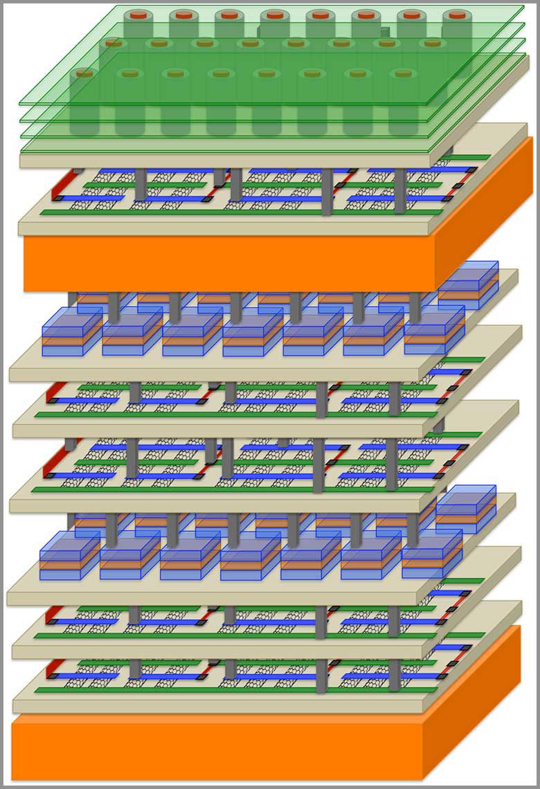
- Stanford University researchers discussing a monolithic 3D AI chip emphasize that by “drastically shortening data movement and adding many more vertical pathways, the chip can achieve both higher throughput and lower energy per operation,” underscoring why 3D architectures are strategically attractive for AI startups. [lyvgf0]
- A reference on on‑chip communication calls it “a comprehensive reference on concepts, research and trends in on-chip communication architecture design,” reflecting how architects now treat interconnect and networks‑on‑chip as first‑class parts of the chip architecture. [t14wm9]
- Policy researchers studying “Chip Architectures Under Advanced Computing Sanctions” describe their work as the “first study on the architectural and economic externality implications” of sanctions, showing that architectural choices now intersect directly with trade and regulatory strategy. [st4bw4]
Common Misuses
- Using “chip architecture” when you mean manufacturing nodeMany marketing materials conflate moving from, say, 7 nm to 3 nm with “a new chip architecture,” when this is a process‑technology change; the more precise term is process node or technology node, while “architecture” should refer to the organization of compute, memory, and interconnect. [lyvgf0] [jxot1z] [t14wm9]
- Calling any software‑visible change “a new architecture”Adding a few instructions or firmware features on top of an existing Arm or x86 design is often described as “a new architecture,” but it is usually an extension of an existing ISA or a microarchitectural revision, not a fundamentally new chip architecture. [l04l7i] [v18ogx]
- Labeling a single accelerator block as “our whole chip architecture”Startups sometimes market a new matrix unit or NPU core as “a novel chip architecture,” when in fact the broader SoC still relies on conventional CPU, memory hierarchy, and interconnect; the correct term is accelerator design or compute core design, within a mostly standard SoC architecture. [98hxl9] [tmoau5] [jxot1z]