Write a comprehensive one-page article about "Gate-all-around FET".
Model: sonar-pro
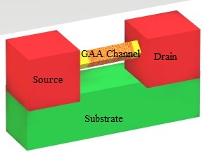
Gate-all-around Field-Effect Transistor (GAAFET) is an advanced transistor architecture where the gate electrode completely surrounds the semiconductor channel on all sides, enabling unprecedented control of current flow and significantly reducing leakage. As Moore's Law continues to push the boundaries of miniaturization, GAAFETs have emerged as a critical solution to sustain high performance and efficiency in semiconductor devices at and below the 3nm technology node, replacing previous FinFET architectures.
[b6zncn]
[lag09l]
[w5dms3]
Detailed Explanation and Concept
A GAAFET is fundamentally different from traditional planar and FinFET transistor structures. While FinFETs surround the channel on three sides, the gate in a GAAFET wraps around all four sides of the channel—typically implemented as horizontal stacks of nanosheets or nanowires made from silicon or other semiconductors. This architecture maximizes electrostatic control, enabling better modulation of current and reducing short-channel effects that plague smaller transistor designs.
[60yt7c]
[lag09l]
[w5dms3]
For example, in a GAAFET, the source and drain are positioned at either end of the horizontal nanosheet or nanowire, with a high-k dielectric and the gate material wrapping the structure completely. Applying a voltage to the gate modulates the current through the channel more efficiently than previous transistor types. This improved control is crucial in modern integrated circuits, especially as device dimensions shrink into the sub-5nm regime.
[60yt7c]
[k83wci]
Practical Examples and Use Cases
GAAFETs are already being deployed in the most advanced semiconductor products:
High-performance computing (HPC) processors, where density and power efficiency are critical.
Mobile processors—for smartphones and tablets—benefit from lower power consumption and less heat generation.
Artificial intelligence (AI) accelerators and automotive chips, where both speed and reliability at tiny geometries are vital.
[b6zncn]
[lag09l]
[shgc0s]
For instance, Samsung's 3nm process node, first introduced commercially in 2022, uses GAAFETs (branded as MBCFET) to increase performance and reduce power beyond what was achievable with FinFETs.
[b6zncn]
[shgc0s]
Benefits and Applications
Key benefits of GAAFETs include:
Superior gate control reduces leakage current and suppresses short-channel effects, extending transistor scaling further than previous technologies.
Enhanced performance and lower power consumption due to more effective channel control.
Design flexibility: Drive current can be precisely tuned by adjusting nanosheet width and stacking layers.
[lag09l]
[w5dms3]
Higher device density on chips, making them ideal for ultra-compact, high-speed applications.
[60yt7c]
[b6zncn]
These advantages make GAAFETs especially relevant for next-generation CPUs, GPUs, SoCs, AI chips, and other logic devices that require extreme miniaturization and efficiency.
[lag09l]
[shgc0s]
Challenges and Considerations
Despite their promise, GAAFETs present manufacturing challenges:
Uniformly wrapping the gate around ultra-thin channels (less than 10nm) demands advanced fabrication techniques.
Integrating new materials like SiGe or III-V compounds introduces complexity.
Maintaining consistent performance and yield across billions of transistors on a single chip is technically demanding.
[60yt7c]
[w5dms3]
[5c0kr1]
Current State and Trends
The industry's transition toward GAAFET technology is well underway, especially for 3nm and sub-3nm nodes. Samsung led the market by introducing GAAFETs for mass production in 2022; Intel (RibbonFET), TSMC, and other major players plan to adopt similar architectures in their forthcoming nodes.
[b6zncn]
[shgc0s]
Key suppliers like Synopsys and Applied Materials are providing the tools and materials to overcome fabrication challenges.
[lag09l]
[w5dms3]
Continued R&D focuses on refining nanosheet/nanowire structures, improving process control, and integrating new channel materials to push performance even further. The trend now is stacking multiple nanosheet layers vertically for even greater transistor density within the same silicon footprint.
[lag09l]
Future Outlook
Looking forward, GAAFETs are expected to enable transistor scaling to the 2nm node and beyond, sustaining the pace of innovation in processors for AI, quantum computing, and internet-of-things (IoT) devices. As fabrication matures and costs decrease, GAAFETs will see broader application, supporting smarter, faster, and more energy-efficient electronics across industries.
[b6zncn]
[w5dms3]
In summary, Gate-all-around FETs represent a decisive leap in transistor technology, offering improved control, performance, and scaling. Their adoption signals a new era of efficiency and innovation in the semiconductor landscape.